

The NVIDIA DGX Spark


The NVIDIA DGX Spark
The NVIDIA DGX Spark represents a watershed moment in accessible AI infrastructure. In 2017, the landmark “Attention is All You Need” paper that introduced the Transformer architecture relied on an eight-GPU P100 server configuration, consuming tens of kilowatt-hours and occupying significant data center real estate. Today, the DGX Spark delivers superior computational performance in a compact 240-watt desktop form factor. This dramatic evolution in power efficiency and form factor compression makes formerly datacenter-exclusive AI capabilities accessible to individual researchers, small teams, and distributed development organizations.
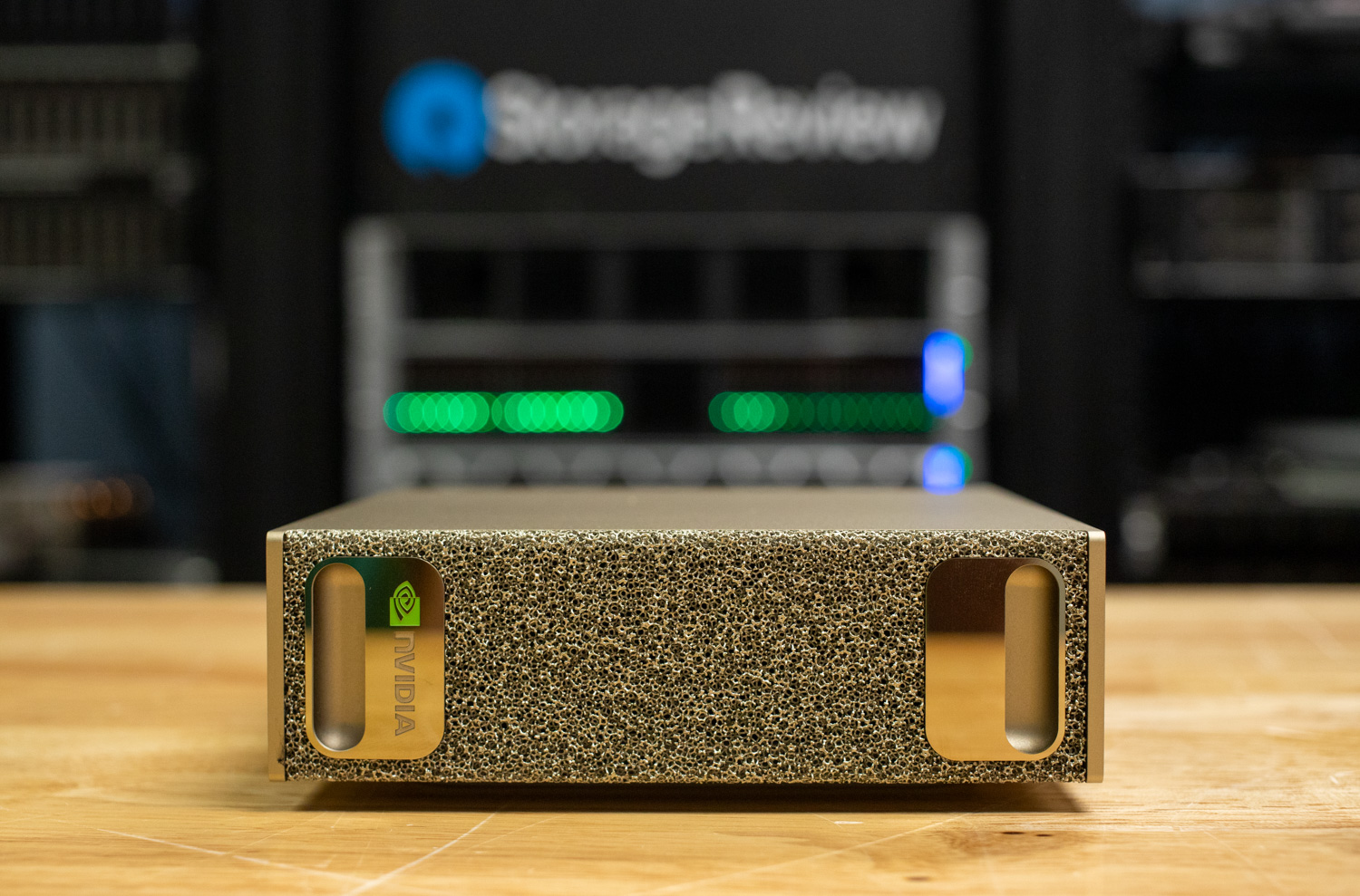
What distinguishes Spark from previous desktop AI solutions is its comprehensive approach to the full development lifecycle. Rather than forcing compromises between experimentation, fine-tuning, and deployment, Spark provides genuine capability across all phases. The 128 GB unified memory architecture enables full parameter fine-tuning of models that would require cloud resources on conventional workstations, while delivering hundreds of tokens per second throughput suitable for batch inference workloads, including synthetic data generation. The inclusion of ConnectX-7 networking with 200Gb fabric capability means organizations can cluster multiple Spark systems for even larger model exploration, though as we’ll demonstrate, even a single unit proves remarkably capable.
Key Takeaways
Datacenter power in a desktop: GB10 Grace Blackwell in a 1.13-liter, 240W box, priced at $3,999, delivering up to 1 petaFLOP FP4 sparse performance.
Memory that changes workflows: 128GB unified memory enables full-parameter fine-tuning of 8B models locally and high-throughput inference. In testing we saw Llama 3.1 8B FP4 reach ~924 tok/s at 128 concurrency, and Qwen3 Coder 30B-A3B FP8 hit ~483 tok/s at batch 64.
Ready to scale and attach fast storage: Integrated ConnectX-7 provides 200G fabric for clustering or NVMe-oF. The internal 2242 Gen5 NVMe is convenient but limited for heavy I/O, so external NVMe-oF over RDMA is the better path for sustained throughput.
Day-one software maturity: Ships with DGX OS, CUDA, cuDNN, TensorRT, AI Workbench, containers, and workflow playbooks so teams can run real workloads immediately.
Proven real-world performance: MAMF measured ~99.8 TFLOPs BF16 and ~207.7 TFLOPs FP8. GDSIO reads peaked ~11.4 GiB/s internally, with higher ceiling expected over the 200G fabric.
What is DGX Spark, and Who Should Consider It?
The NVIDIA DGX Spark is fundamentally a complete AI development platform rather than simply a GPU component. At its core sits the GB10 Grace Blackwell Superchip, which integrates a Blackwell architecture GPU featuring fifth-generation Tensor Cores with a 20-core Arm CPU (10× Cortex-X925 + 10× Cortex-A725) connected via NVLink-C2C. This coherent interconnect architecture, according to NVIDIA, enables up to 5× higher bandwidth compared to PCIe Gen 5, creating a unified computational fabric rather than discrete processing domains.
To get users started, NVIDIA ships DGX OS built on Ubuntu Desktop with the complete AI software stack pre-configured, including CUDA, cuDNN, TensorRT, NVIDIA Container Runtime, and AI Workbench, eliminating the typical driver challenges and environment configuration overhead that plagues custom workstation builds. The system offers flexible deployment paradigms: attach peripherals and use it as a compact workstation with the full Ubuntu desktop experience, or deploy it as a headless network appliance accessible via NVIDIA Sync, which provides seamless integration with JupyterLab, VS Code, Cursor IDE, and SSH terminals.
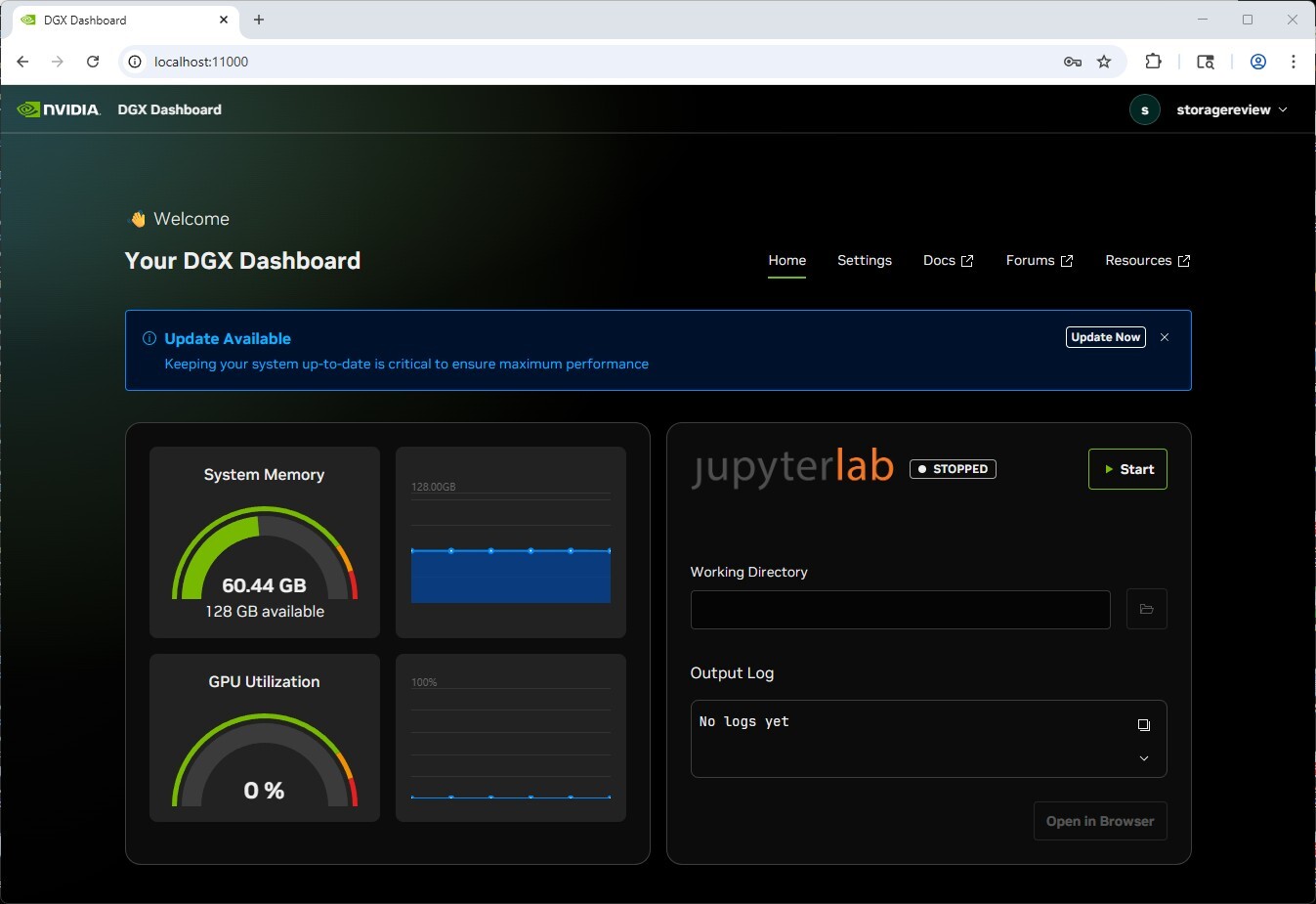
This is purpose-built infrastructure for AI practitioners, researchers fine-tuning language models, data scientists accelerating RAPIDS workflows, developers implementing agentic systems, or teams experimenting with architectures with ablative models at a small scale. Spark targets professionals who need serious AI computational capability without datacenter complexity.
NVIDIA DGX Spark Technical Specifications
| Specification | Details |
|---|---|
| Architecture | |
| GPU | NVIDIA Blackwell Architecture |
| CPU | 20-core Arm (10x Cortex-X925 + 10x Cortex-A725) |
| Tensor Cores | 5th Generation |
| RT Cores | 4th Generation |
| NVENC / NVDEC | 1× / 1× |
| Memory | |
| System Memory | 128 GB LPDDR5X (Unified System Memory) |
| Memory Interface | 256-bit |
| Memory Bandwidth | 273 GB/s |
| Performance | |
| FP4 | up to 1 petaFLOP (with Sparsity) |
| Storage | |
| Storage | 1 TB or 4 TB NVMe M.2 (Self-encrypted) |
| Connectivity | |
| USB | 4× Type-C USB 3.2 Gen 2×2 (20Gbps) |
| Ethernet | 1× 10GbE RJ-45 |
| NIC | ConnectX-7 Smart NIC – 2x 200G QSFP (Allows for a maximum of 200G bandwidth) |
| Wireless | Wi-Fi 7, Bluetooth 5.3 |
| Audio Output | HDMI Multichannel Audio Output |
| Display Connectors | 1× HDMI 2.1a |
| Mechanical | |
| Dimensions | 150 × 150 × 50.5 mm (5.9 × 5.9 × 1.98″) |
| Weight | 1.2 kg |
| Power Consumption | 240 W |
NVIDIA DGX Spark Design & Build
The NVIDIA DGX Spark continues NVIDIA’s unmistakable industrial design language, featuring a compact chassis that mirrors the look and feel of its larger DGX systems. The front panel features miniature hand-hold cutouts, a nod to the original full-sized DGX units’ handles, and a gold-speckled metallic finish that delivers a refined, premium texture, accented by NVIDIA’s iconic green logo badge.
Physically, the DGX Spark measures 5.9 × 5.9 × 1.98 inches (150 × 150 × 50.5 mm) and weighs 2.6 pounds (1.2 kg), giving it a total internal volume of 1.13 liters. This places it firmly within the 1-liter small-form-factor PC class. Despite its minimal footprint, the system feels dense and robust thanks to an all-metal alloy shell that also serves as a passive heat spreader, maintaining focus on both form and function.
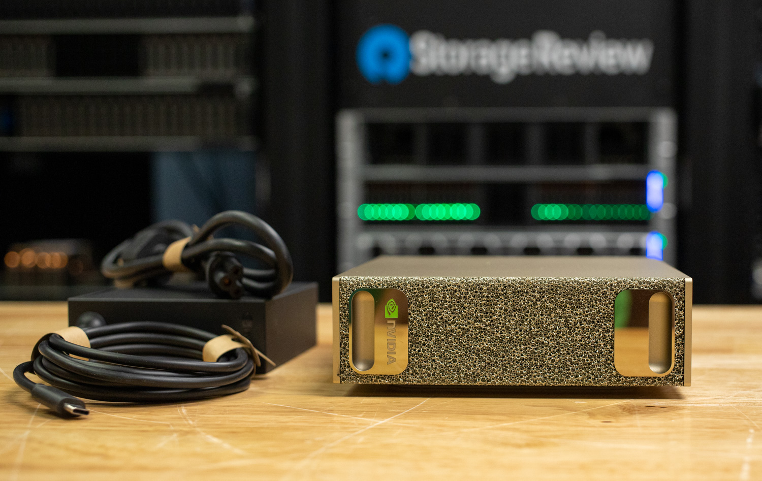
Power is provided by a 240 W USB-C external power brick, seen beside the main unit in the image. The brick is compact and well-built, using a standard C5 (cloverleaf) connector for AC input and matching the DGX Spark’s clean, efficient design.
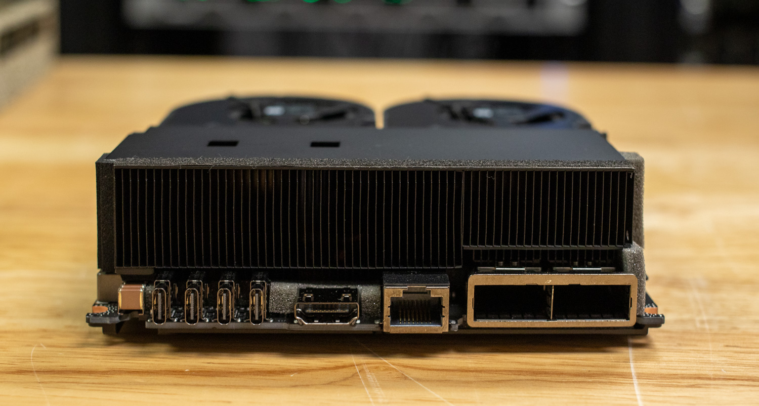
Turning to the rear, the DGX Spark carries over the same gold-speckled textured finish seen on the front, maintaining a cohesive design throughout the chassis. Starting from the left, the power button sits beside four USB-C ports, one of which provides Power Delivery for the unit. These are followed by a single HDMI 2.1a output, a 10 GbE RJ-45 port, and what makes this unit interesting is the dual 200 GbE QSFP56 interfaces driven by an integrated NVIDIA ConnectX-7 SmartNIC.
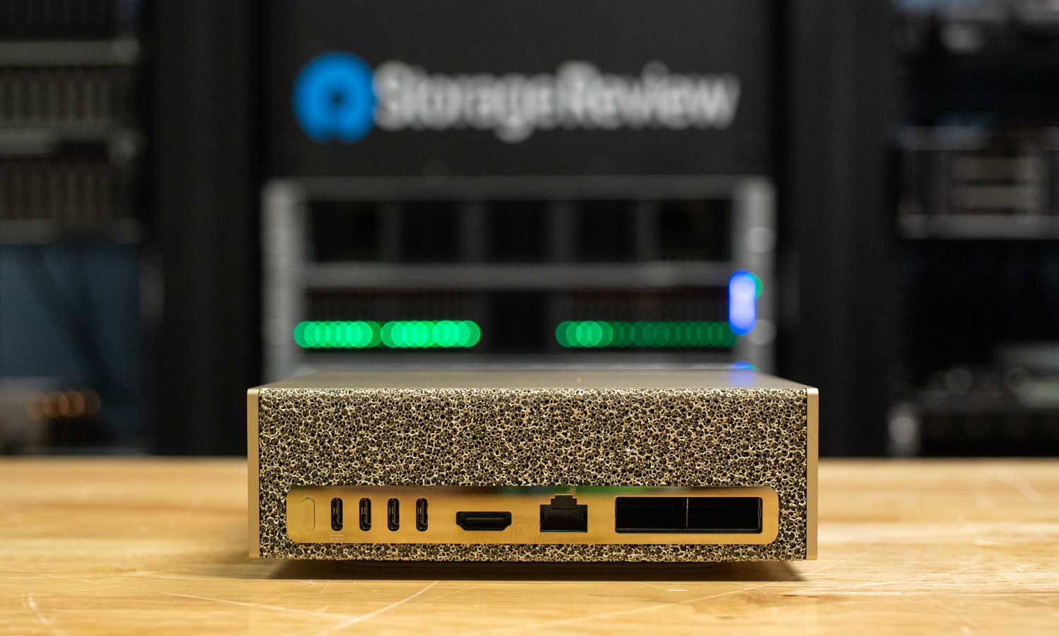
At first glance, you might deduce that the Spark allows for 400G of connectivity; unfortunately, due to PCIe limitations, the Spark is only able to provide 200G of connectivity. Wanting to know more, we dug deeper into the topology of the Spark:
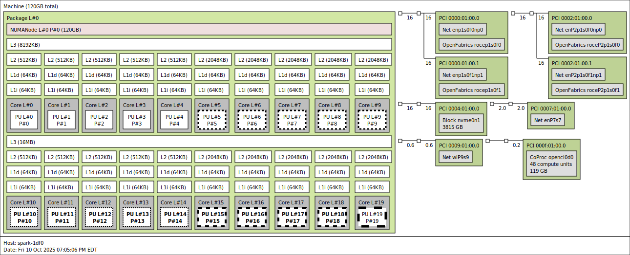
Using lstopo, we observe the two interconnects from the CX7 NIC. Electrically, the CX7 is connected via two Gen5 x4 links. Within the OS, these connections appear as four interfaces, each supporting a maximum bandwidth of 200G. Due to limited test time, we were unable to discover all networking quirks of this platform outside of our NVMe-oF tests, which are detailed later in the article. However, we plan to explore this platform further and will release future articles that dive deeper into its capabilities, like clustering multiple sparks together for a mini cluster.
Looking into other connected devices, next up is the tiny 2242 form factor M.2 SSD connected with Gen5 x4, followed by the Realtek RJ45 10GbE controller connected with PCIe Gen4 x1 link, and the MediaTek Wi-Fi Controller connected with a PCIe Gen3 x1 link.
Diving into the CPU, the Spark contains a 20-core Arm processor with a heterogeneous big little architecture, similar to Intel’s latest processors, consisting of 10 Cortex-A725 efficiency cores and 10 Cortex-X925 performance cores split across two L3 cache clusters. The first cluster (8MB L3) contains CPUs 0-4 (Cortex-A725, max 2808 MHz) and CPUs 5-9 (Cortex-X925, max 3900 MHz), while the second cluster (16MB L3) contains CPUs 10-14 (Cortex-A725, max 2860 MHz) and CPUs 15-19 (Cortex-X925, max 3978-4004 MHz). Each core has private 64KB L1 data and 64KB L1 instruction caches, but the L2 cache differs significantly by core type: the efficiency Cortex-A725 cores have 512KB L2 caches, while the performance Cortex-X925 cores have substantially larger 2MB L2 caches (4× larger). The fastest cores are CPUs 15-19, which benefit from both the larger 16MB L3 cache and higher frequencies, with CPU 19 being the peak performance core at 4004 MHz. These different power/frequency levels are signified by the dashed lines on the core on the topology shown above.
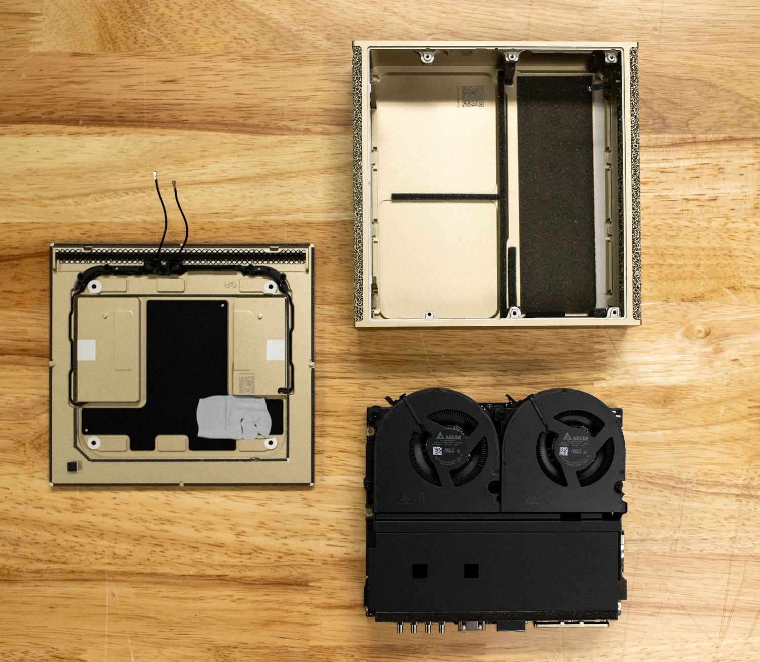
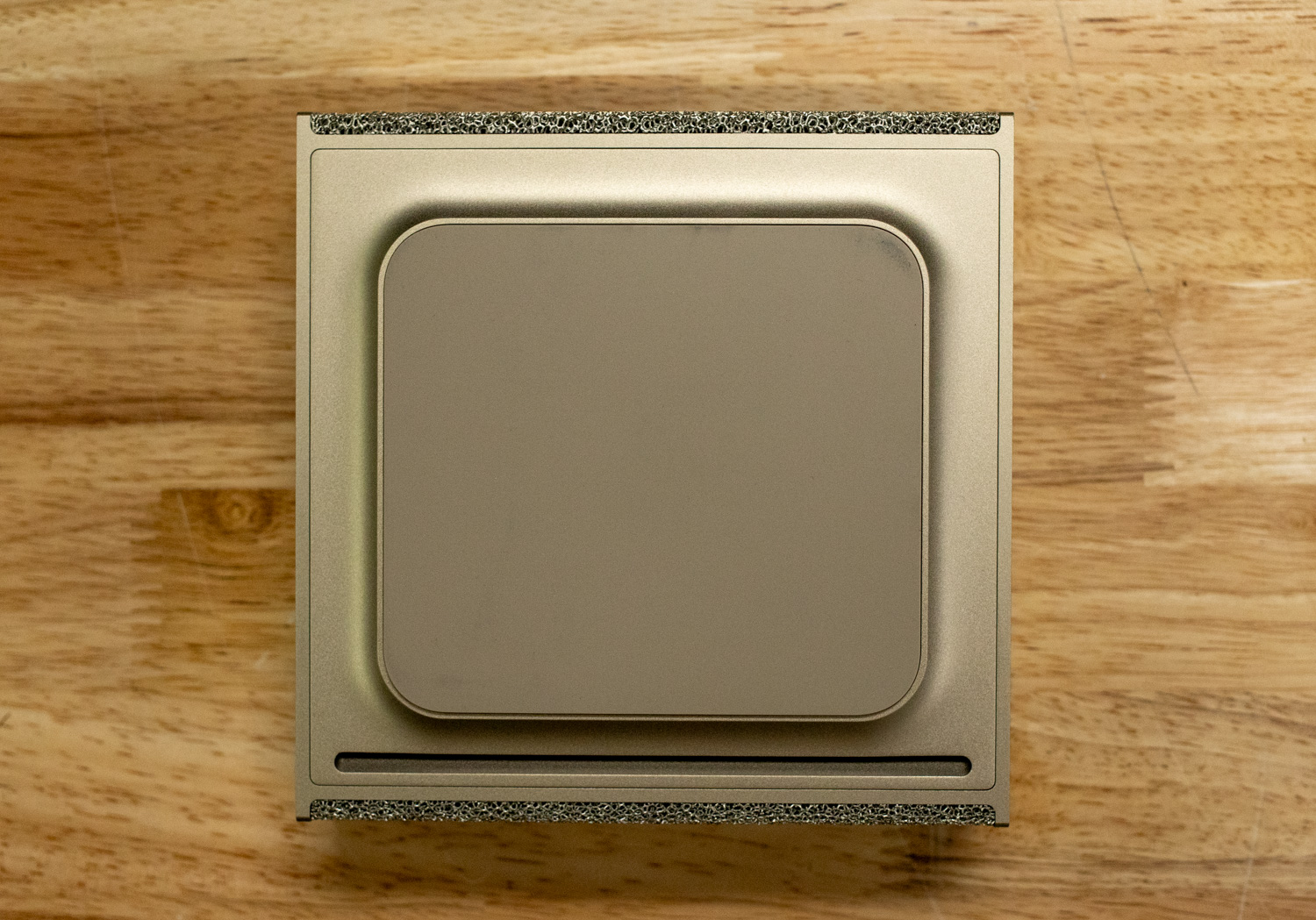
Zooming back out, we flip the DGX Spark over; the only visible plastic component is the base cover, which attaches magnetically to the bottom of the chassis. This design keeps the exterior clean while allowing for quick access to the internals. Once the magnetic base is removed, four screws are exposed, granting access to the main internal compartment.
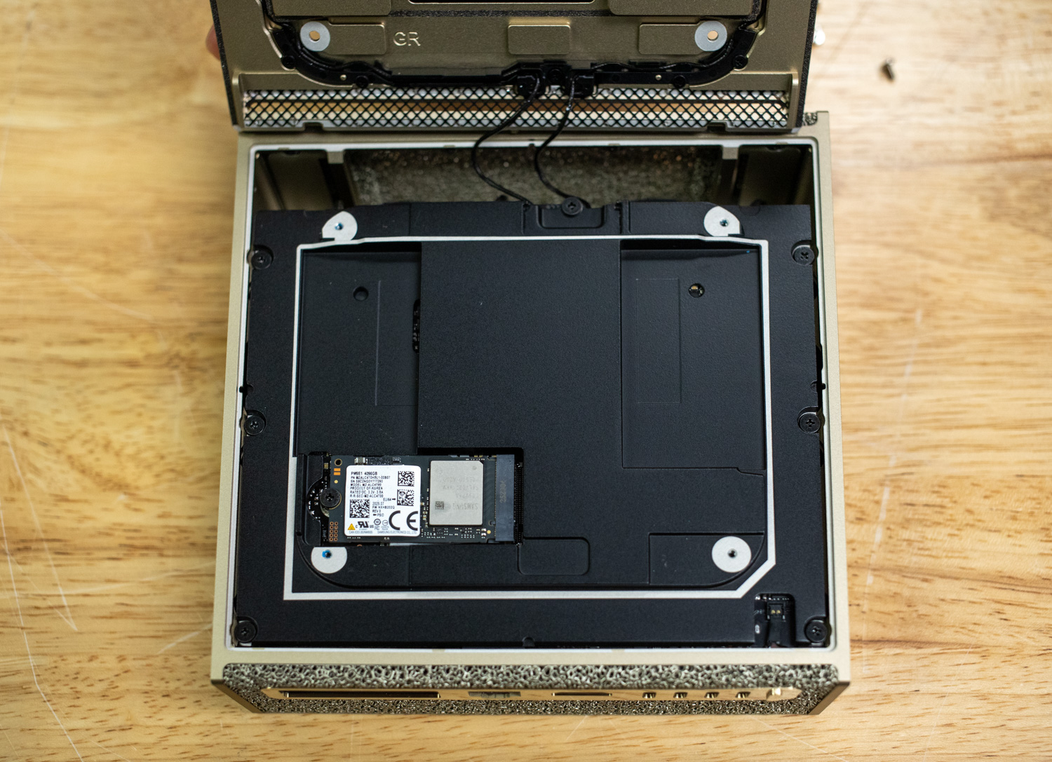
Inside, we can see antenna wiring routed toward the top section of the unit, confirming the inclusion of Wi-Fi 7 and Bluetooth 5.3 connectivity. This provides flexible network options, particularly useful for mobile or lab deployments where wired access may not be available.
Also visible is the unit’s storage solution, a PCIe Gen5 2242 M.2 SSD, a less-common form factor for such high-performance hardware. The configuration shown here includes a 4TB Samsung NVMe drive in our configuration.
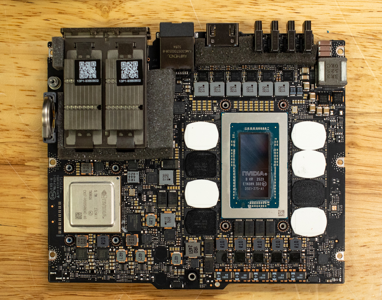
Diving deeper into the DGX Spark reveals the heart of the system, the NVIDIA Grace Blackwell’s GB10 Superchip. Flanking the GB10 Superchip are the 8 soldered LPDDR5X unified system memory delivering 273 GB/s of bandwidth, ensuring fast data access across both CPU and GPU operations.
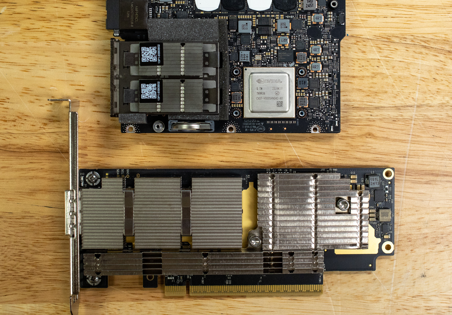
Right next to the chip is the CX7 NIC, which, as previously mentioned, provides 200G of connectivity. This allows users to connect the Spark to high-speed storage or even cluster multiple instances of the Spark together. NVIDIA has validated and sells a cluster of 2 Sparks that can be directly connected to support even bigger AI models.
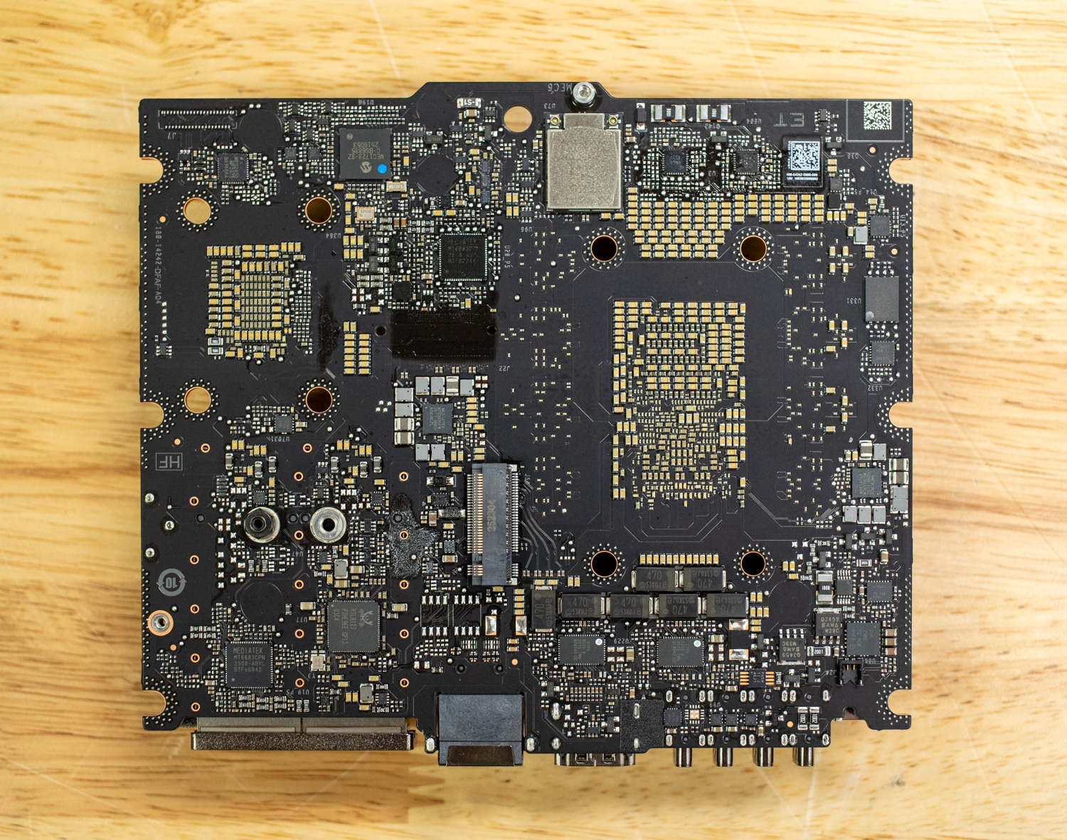
Finally, flipping the board over reveals all the PCIe connectivity, including the PCIe Gen5 x4 2242 M.2 SSD and the PCIe Gen3x1 MediaTek Wi-Fi adapter.
Where Spark Becomes Indispensable: The Modern AI Development Appliance
The DGX Spark proves particularly compelling across several distinct professional contexts, each benefiting from its unique combination of unified memory, compact form factor, and comprehensive software integration.
Data Science Acceleration: From Pandas to Production
For data scientists, the NVIDIA DGX Spark represents a big improvement in workflow velocity and experience. The ConnectX-7 networking delivering 200 Gbps bandwidth, combined with CUDA X accelerated libraries, transforms data preprocessing. AI and Data Science are built on the foundation of good data in, good data out. Traditionally, the most time-consuming phase of any conventional ML project is data cleaning and feature extraction. Conventional workflows typically involve loading datasets into tools like pandas and performing transformations on CPU cores, which is generally slow. Manual exploration and feature engineering can also be a significant blocker. Spark enables end-to-end GPU acceleration through RAPIDS.
A typical enterprise data science scenario involves feature engineering on datasets in the 40-80GB range: joining multiple tables, computing aggregations across temporal windows, handling categorical encoding, and normalizing distributions. On CPU infrastructure, this preprocessing might consume hours. With RAPIDS cuDF loading the entire dataset into Spark’s 128 GB unified memory, these operations complete in minutes at 10× or higher acceleration. The subsequent model training benefits equally whether classical ML with cuML or deep learning with PyTorch, eliminating the traditional bottleneck where data scientists wait on infrastructure rather than iterating on hypotheses.